Introduction
PCB Design Software is the lifeblood of modern electronics engineering. It empowers engineers and designers to turn circuit schematics into real-world boards, validate designs before fabrication, and optimize for high-speed, multi-layer, and mixed-signal systems. With electronics pushing the limits in IoT, automotive, aerospace, and consumer devices, these tools are no longer optional—they’re essential for precision, speed, and reliability.
Modern platforms offer AI-assisted routing, real-time signal/power analysis, 3D visualization, cloud collaboration, and manufacturing integration, helping teams innovate faster and reduce costly errors. With the right PCB design software, even complex boards can be designed efficiently, verified thoroughly, and manufactured reliably.
Common Use Cases
- Designing multi-layer, high-speed PCBs for automotive and aerospace
- Consumer electronics and IoT hardware development
- Industrial control and automation electronics
- Power electronics and mixed-signal devices
- High-frequency RF and microwave circuit boards
Key Criteria for Buyers
- Schematic capture and PCB layout capabilities
- Advanced routing (manual and auto-routing)
- Design rule checking (DRC) and manufacturing validation
- Signal integrity, power integrity, and thermal analysis
- 3D visualization and MCAD integration
- BOM management and fabrication output
- Collaboration and version control
- Multi-layer and high-density PCB support
- Licensing flexibility (subscription vs perpetual)
- Integration with simulation and fabrication workflows
Best for: Electronics engineers, hardware designers, PCB specialists, and R&D teams who need precise, validated boards and efficient production-ready outputs.
Not ideal for: Hobbyists or teams needing only simple boards, where lightweight or open-source tools are sufficient.
Key Trends in PCB Design Software
- AI-assisted auto-routing speeds layout and reduces errors
- Cloud collaboration allows distributed teams to work seamlessly
- Real-time signal/power integrity analysis built into layout workflows
- 3D visualization and MCAD integration ensures mechanical fit
- Support for high-speed and differential pair routing
- Constraint-driven design rules improve manufacturability
- Version control and team workflows enable design coordination
- Automated fabrication outputs for faster production
- Component libraries and design reuse streamline engineering cycles
- Subscription-based and scalable licensing for teams of all sizes
How We Selected These Tools (Methodology)
- Reviewed market adoption and global usage
- Evaluated feature breadth from schematic to manufacturing output
- Assessed signal/power/thermal analysis and high-speed capabilities
- Checked collaboration and cloud readiness
- Considered ease of use for engineers and designers
- Balanced enterprise vs mid-market vs accessible tools
- Verified active development and vendor support
- Examined integration with MCAD, simulation, and fabrication workflows
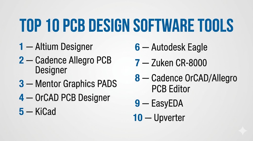
Top 10 PCB Design Software Tools
#1 — Altium Designer
Short description: A versatile, high-powered PCB design platform combining schematic capture, board layout, real-time validation, and cloud collaboration for enterprise teams.
Key Features
- Unified schematic and PCB layout environment
- Constraint-driven routing
- Real-time 3D visualization
- Signal and power integrity analysis
- BOM management and fabrication output
- Cloud collaboration for team design
Pros
- Powerful all-in-one workflow
- Suitable for complex, high-density boards
Cons
- Expensive for small teams
- Steep learning curve
Platforms / Deployment
Windows / Cloud
Security & Compliance
Not publicly stated
Integrations & Ecosystem
- MCAD co-design
- Vendor part libraries
- Fabrication interfaces
Support & Community
Global enterprise support and an active community of engineers.
#2 — Cadence Allegro PCB Designer
Short description: Enterprise-grade platform for high-speed, multi-layer boards with advanced signal integrity and manufacturing validation.
Key Features
- Advanced routing and layout tools
- Signal and power integrity analysis
- Multi-user collaboration
- High-speed and RF design support
- BOM and fabrication output
Pros
- Excellent for mission-critical designs
- Strong verification and manufacturing workflow
Cons
- Premium pricing
- Requires skilled designers
Platforms / Deployment
Windows / Linux
Security & Compliance
Not publicly stated
Integrations & Ecosystem
- PLM and simulation tools
- Fabrication output standards
- Design verification workflows
Support & Community
Enterprise support with comprehensive documentation.
#3 — Mentor Graphics PADS
Short description: Mid-market PCB design software balancing usability with advanced layout, verification, and manufacturing support.
Key Features
- Schematic capture and PCB layout
- Constraint-driven DRC
- Signal integrity analysis
- BOM management
- Thermal analysis and library management
Pros
- User-friendly for small to mid-sized teams
- Solid design-to-manufacturing workflow
Cons
- Limited high-speed capabilities
- Less suitable for enterprise-scale designs
Platforms / Deployment
Windows
Security & Compliance
Not publicly stated
Integrations & Ecosystem
- Component libraries
- Fabrication output
- MCAD integration
Support & Community
Vendor-supported with robust SMB documentation.
#4 — OrCAD PCB Designer
Short description: Popular PCB design tool with schematic capture, layout, and rule-driven validation for SMB teams and mid-market designs.
Key Features
- Schematic capture and layout
- Rule-based design constraints
- Signal integrity checks
- BOM automation
- Fabrication file output
Pros
- Accessible pricing
- Streamlined workflow for smaller teams
Cons
- Limited 3D and high-speed analysis
- Less scalable for enterprise boards
Platforms / Deployment
Windows
Security & Compliance
Not publicly stated
Integrations & Ecosystem
- Libraries and templates
- Manufacturing output
- Simulation tools
Support & Community
Active vendor support and documentation.
#5 — KiCad
Short description: Open-source PCB design suite with schematic capture, layout, and basic analysis, widely used by hobbyists and SMB teams.
Key Features
- Free and open-source
- 3D board visualization
- Schematic capture and PCB layout
- BOM and fabrication export
- Community libraries
Pros
- No license cost
- Strong open-source community
Cons
- Limited analysis features
- Less polished workflow than commercial tools
Platforms / Deployment
Windows / macOS / Linux
Security & Compliance
Not publicly stated
Integrations & Ecosystem
- Community libraries
- Export formats for fabrication
- 3D visualization plugins
Support & Community
Active open-source community.
#6 — Autodesk Eagle
Short description: User-friendly PCB tool for makers and SMB teams with cloud collaboration and schematic/PCB layout integration.
Key Features
- Intuitive schematic editor
- Auto-routing and manual layout
- Cloud project storage and collaboration
- BOM and fabrication output
- Community part libraries
Pros
- Accessible for beginners and small teams
- Cloud-enabled collaboration
Cons
- Limited enterprise features
- Moderate analysis depth
Platforms / Deployment
Windows / macOS / Linux / Cloud
Security & Compliance
Not publicly stated
Integrations & Ecosystem
- Autodesk cloud libraries
- BOM export
- Community-driven designs
Support & Community
Strong online community and tutorials.
#7 — Zuken CR‑8000
Short description: High-end system-level PCB platform for complex electronics with multi-board and high-speed workflows.
Key Features
- Multi-board design support
- Constraint-driven routing
- Signal integrity and thermal analysis
- High-speed routing
- Team collaboration and version control
Pros
- Ideal for complex, large-scale designs
- Enterprise-grade workflow support
Cons
- High cost
- Steep learning curve
Platforms / Deployment
Windows
Security & Compliance
Not publicly stated
Integrations & Ecosystem
- MCAD co-design
- PLM integration
- Simulation connectors
Support & Community
Enterprise support with professional training.
#8 — Cadence OrCAD/Allegro PCB Editor
Short description: Flexible PCB solution scaling from mid-market to enterprise with unified constraint management.
Key Features
- Seamless OrCAD-to-Allegro workflow
- Constraint-driven routing
- High-speed design support
- SI/PI and verification tools
- BOM and manufacturing output
Pros
- Scales with team growth
- Strong data management and verification
Cons
- Cost grows with capability
- Requires learning time for full enterprise use
Platforms / Deployment
Windows / Linux
Security & Compliance
Not publicly stated
Integrations & Ecosystem
- Simulation suites
- PLM systems
- Fabrication tools
Support & Community
Professional vendor support available.
#9 — EasyEDA
Short description: Browser-based PCB tool for makers, students, and light professional use.
Key Features
- Web-based schematic capture and layout
- Component libraries
- BOM export
- Fabrication output
- Community project sharing
Pros
- No installation
- Accessible for beginners
Cons
- Limited analysis
- Not enterprise-grade
Platforms / Deployment
Web / Cloud
Security & Compliance
Not publicly stated
Integrations & Ecosystem
- Cloud libraries
- Fabrication output
- Community-driven designs
Support & Community
Active tutorials and user forums.
#10 — Upverter
Short description: Cloud-native collaborative PCB platform for distributed teams.
Key Features
- Browser-based schematic and layout
- Real-time team collaboration
- Component management
- Version control
- Manufacturing outputs
Pros
- Ideal for distributed teams
- Minimal setup
Cons
- Limited advanced PCB analysis
- Cloud dependency
Platforms / Deployment
Web / Cloud
Security & Compliance
Not publicly stated
Integrations & Ecosystem
- Cloud libraries
- Manufacturing export
- Real-time collaboration
Support & Community
Vendor-supported with growing community.
Comparison Table
| Tool Name | Best For | Platform(s) | Deployment | Standout Feature | Public Rating |
|---|---|---|---|---|---|
| Altium Designer | Enterprise PCB & collaboration | Win/Cloud | Hybrid | Unified ECAD | N/A |
| Cadence Allegro | High-speed complex boards | Win/Linux | Hybrid | Constraint-driven routing | N/A |
| Mentor PADS | Mid-market PCB | Windows | Local | Layout + verification | N/A |
| OrCAD PCB Designer | SMB PCB | Windows | Local | Rule-driven design | N/A |
| KiCad | Hobbyists & SMB | Win/macOS/Linux | Local | Open-source | N/A |
| Autodesk Eagle | Makers & SMB | Win/macOS/Linux | Cloud | Cloud collaboration | N/A |
| Zuken CR‑8000 | System-level multi-board | Windows | Local | System-level workflow | N/A |
| OrCAD/Allegro PCB | Scalable ECAD | Win/Linux | Hybrid | Constraint management | N/A |
| EasyEDA | Makers & students | Web/Cloud | Cloud | Browser-based | N/A |
| Upverter | Collaborative cloud PCB | Web/Cloud | Cloud | Real-time team collaboration | N/A |
Evaluation & Scoring of PCB Design Software
| Tool | Core | Ease | Integrations | Security | Performance | Support | Value | Weighted Total |
|---|---|---|---|---|---|---|---|---|
| Altium Designer | 10 | 7 | 10 | 6 | 9 | 9 | 7 | 8.4 |
| Cadence Allegro | 10 | 6 | 9 | 6 | 10 | 8 | 6 | 8.1 |
| Mentor PADS | 8 | 8 | 7 | 6 | 8 | 8 | 7 | 7.6 |
| OrCAD | 8 | 8 | 7 | 6 | 8 | 8 | 7 | 7.6 |
| KiCad | 6 | 7 | 6 | 5 | 7 | 7 | 10 | 7.1 |
| Eagle | 7 | 8 | 6 | 5 | 7 | 8 | 8 | 7.4 |
| Zuken CR‑8000 | 9 | 6 | 9 | 6 | 9 | 8 | 6 | 7.9 |
| OrCAD/Allegro PCB | 9 | 7 | 9 | 6 | 8 | 8 | 7 | 8.0 |
| EasyEDA | 5 | 9 | 5 | 5 | 6 | 7 | 8 | 7.0 |
| Upverter | 6 | 9 | 6 | 5 | 6 | 7 | 8 | 7.1 |
Which PCB Design Software Tool Is Right for You?
Solo / Freelancer
- KiCad → free, robust, and flexible
- EasyEDA → browser-based and easy to start
SMB
- OrCAD PCB → balanced workflow and value
- Autodesk Eagle → accessible for small teams
Mid-Market
- Mentor PADS → advanced features for growing teams
- OrCAD/Allegro → scalable ECAD solution
Enterprise
- Altium Designer → unified, full-featured platform
- Cadence Allegro → high-speed, mission-critical boards
Budget vs Premium
- Budget: KiCad, EasyEDA
- Premium: Altium Designer, Zuken CR‑8000
Feature Depth vs Ease of Use
- Deep: Allegro, Altium, Zuken
- Easy: Eagle, Upverter, EasyEDA
Integrations & Scalability
- Enterprise: Altium Designer, Allegro
- Small teams: Eagle, PADS
Security & Compliance Needs
- Cloud tools require governance; most platforms do not publicly state compliance.
Frequently Asked Questions (FAQs)
1. What is PCB design software?
It allows designers to create, verify, and prepare printed circuit boards for manufacturing.
2. Which PCB tool is easiest for beginners?
KiCad, EasyEDA, or Autodesk Eagle are ideal starting points.
3. Can PCB software handle high-speed boards?
Yes, tools like Cadence Allegro, Zuken CR‑8000, and Altium Designer specialize in high-speed and RF layouts.
4. Is PCB software expensive?
Enterprise-grade tools are costly; open-source and cloud-based solutions are more affordable.
5. Do PCB tools include analysis?
Many include signal/power integrity, thermal simulation, and high-speed checks.
6. What is auto-routing?
Automatic trace placement that follows design rules, speeding layout while reducing errors.
7. Can PCB software integrate with MCAD?
Yes, leading platforms allow ECAD-MCAD co-design for mechanical fit verification.
8. Are cloud PCB tools reliable?
Yes, cloud tools like EasyEDA and Upverter provide collaboration but depend on internet connectivity.
9. How hard is learning PCB software?
Varies; beginner tools are quick to pick up, enterprise-grade platforms require training.
10. Should I prioritize ease of use or features?
Design teams may prioritize usability, whereas enterprise teams often require depth and analysis.
Conclusion
PCB Design Software drives modern electronics innovation. From enterprise platforms like Altium Designer and Cadence Allegro to accessible tools like KiCad, Eagle, and EasyEDA, there is a solution for every team size, budget, and complexity level. Cloud tools accelerate collaboration, while enterprise tools deliver high-speed, high-density board design capabilities. Your ideal choice depends on workflow, skillset, and manufacturing needs. Shortlist 2–3 tools, test real designs, and validate workflow, simulation, and fabrication integration before committing. Make your PCB design smarter, faster, and production-ready.
Find Trusted Cardiac Hospitals
Compare heart hospitals by city and services — all in one place.
Explore Hospitals